
- 雷电竞官网登录
- Power Management
- rayapp
- L竞技
- Sensors
- Lighting
- Custom Mixed-Signal ICs (ASICs)
- Power Conversion
- Power Switching
- Memory
- Silicon IP
- GreenPAK Configurable Mixed-Signal
- Timing
- Communications
- IO-Link
- Industrial and Automotive ASICs
- Industrial Edge Computing
- IOX Expansion Module
- IzoT Commissioning Tool (CT)
- IzoT Net Server
- IzoT SDK 2
- IzoT ShortStack SDK
- LNS DDE Server
- LON Upgrade
- LonScanner FX Protocol Analyzer
- Smart Edge Platform
- SmartServer IoT
- SmartServer IoT™ Partner Program
- SmartServer™ IoT Edge Server
- U10 USB Network Interface
- U20 USB Network Interface
- U60 DIN USB Expansion Modules
- U60 FT USB Network Interface Module
- U70 PL-20 USB Network Interface
- Current Control
- Motor Control
- Display
- Modules
- Longevity Program
- Product Selector
- Document Search
- 雷竞技安卓下载
- Application Solution Diagrams
- Connected Health
- Connected Consumer
- Connected rechargeable E-cigarette
- True Wireless Stereo
- USB Type-C ANC Headset
- Beacon, Tracker, Findable
- DECT Ambient Noise Cancellation (ANC) Headset
- Rechargeable E-Cigarette
- Game Controller
- Feature-rich Rechargeable E-Cigarette
- Rechargeable Game Controller
- Bluetooth ANC Headset
- Toothbrush
- Electric MP3 toothbrush
- Voice RCU
- Animal Tracker / Location Tracker
- POS Terminals
- Wall-to-Battery & Direct Charging
- Smart Home
- Smart Appliances
- Industrial & Infrastructure
- Smart Lighting
- Wearables
- Configurable Mixed-signal IC Solutions
- Smart Home
- Home Appliances
- Networking
- Automotive
- Industrial
- Smart Meters
- SoC PMIC Solutions
- Communications
- Connected Medical
- Transportation
- Application Solution Diagrams
- Support
- 雷电竞下载app
You are here
I2C电平位移器

I2C电平位移器
Communication Protocols Application

I2C level-shifters allow two I2C-enabled devices to communicate to each other across two different voltage levels. The given example level shifts from 3.3V to 1.8V.
Necessary Components
- Any GreenPAK
- Four resistors

GreenPAK Diagram
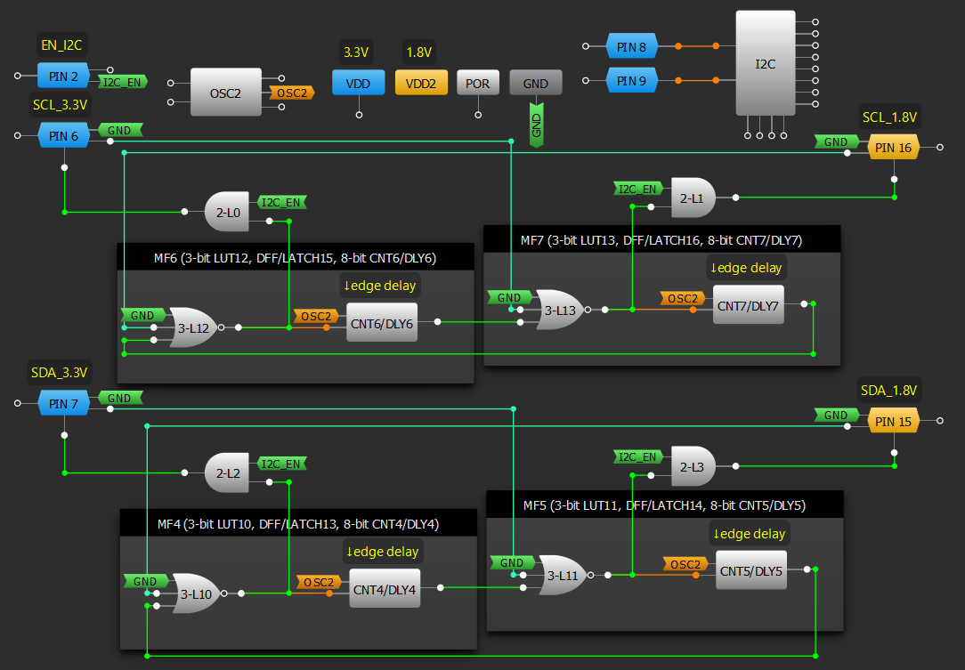
Design Steps
- Configure four GPIO pins as digital input/outputs with the output mode set to open drain NMOS.
- Configure one pin as a digital input for the enable signal.
- Add an AND gate to each input/output.
- Configure four multi-function blocks (or four LUTs and four CNT/DLY blocks if Multi-function blocks aren’t available) as a NOR gate feeding into a falling edge delay.
- Select OSC2 as the clock source for the delay blocks and set it to“Force Power On.”
Resources
GreenPAK Designer files
- I2C电平位移器(5.04 KB)