
- 雷电竞官网登录
- Power Management
- rayapp
- L竞技
- Sensors
- Lighting
- Custom Mixed-Signal ICs (ASICs)
- Power Conversion
- Power Switching
- Memory
- Silicon IP
- GreenPAK Configurable Mixed-Signal
- Timing
- Communications
- IO-Link
- Industrial and Automotive ASICs
- Industrial Edge Computing
- IOX Expansion Module
- IzoT Commissioning Tool (CT)
- IzoT Net Server
- IzoT SDK 2
- IzoT ShortStack SDK
- LNS DDE Server
- LON Upgrade
- LonScanner FX Protocol Analyzer
- Smart Edge Platform
- SmartServer IoT
- SmartServer IoT™ Partner Program
- SmartServer™ IoT Edge Server
- U10 USB Network Interface
- U20 USB Network Interface
- U60 DIN USB Expansion Modules
- U60 FT USB Network Interface Module
- U70 PL-20 USB Network Interface
- Current Control
- Motor Control
- Display
- Modules
- Longevity Program
- Product Selector
- Document Search
- 雷竞技安卓下载
- Application Solution Diagrams
- Connected Health
- Connected Consumer
- Connected rechargeable E-cigarette
- True Wireless Stereo
- USB Type-C ANC Headset
- Beacon, Tracker, Findable
- DECT Ambient Noise Cancellation (ANC) Headset
- Rechargeable E-Cigarette
- Game Controller
- Feature-rich Rechargeable E-Cigarette
- Rechargeable Game Controller
- Bluetooth ANC Headset
- Toothbrush
- Electric MP3 toothbrush
- Voice RCU
- Animal Tracker / Location Tracker
- POS Terminals
- Wall-to-Battery & Direct Charging
- Smart Home
- Smart Appliances
- Industrial & Infrastructure
- Smart Lighting
- Wearables
- Configurable Mixed-signal IC Solutions
- Smart Home
- Home Appliances
- Networking
- Automotive
- Industrial
- Smart Meters
- SoC PMIC Solutions
- Communications
- Connected Medical
- Transportation
- Application Solution Diagrams
- Support
- 雷电竞下载app
You are here
Using DCMP and PWM Macrocell in PWM Mode

Using DCMP and PWM Macrocell in PWM Mode
Pulse-based Control Technique
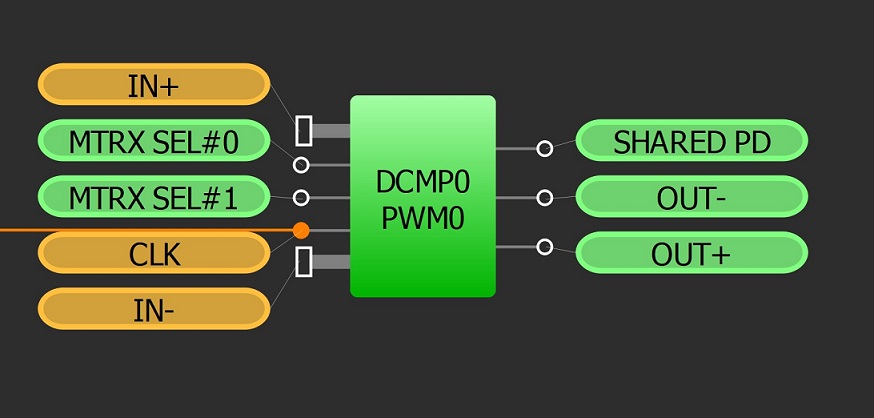
This technique is for the DCMP block, available in the SLG46140, SLG46620, and SLG46621.
The DCMP/PWM block is a special macrocell used to compare two 8-bit values or generated PWM signals. There are three DCMP/PWM blocks per IC that can operate independently, and each DCMP/PWM has two 8-bit inputs (IN+, IN-) that can be used to generate a PWM signal. Inputs MTRX SEL#0 and MTRX SEL#1 are used during static PWM generation to select one of the four available registers, shared amongst the three blocks. Input SHARED PD is used to POWER ON/OFF. The PWM output duty cycle range can be configured to range from 0% to 99.61% or 0.39% to 100%.
Creating the PWM Signal
The PWM generator is similar to a digital comparator, with the exception that the data on one of the inputs is linearly cycling through a set PWM period. The other input is static at a set duty cycle or updating at a very slow rate.
So, to create a PWM signal, we need a PWM ramp source. This is an internal or external counter that counts from 255 down to 0 or vice versa. Another source of data for the DCMP/PWM block should be stable for at least 1 PWM signal period (PWM ramp counter period). It could be data from the SPI, ADC, FSM blocks,orfrom an internal register of DCMP/PWM. Figure 1 shows the operation of a DCMP/PWM when IN- is connected to a CNT/DLY block that counts from 255 down to 0 (PWM ramp counter) and the IN+ source is an internal register set to 250.

Figure1 DCMP/PWM in PWM mode
The IN+ input configurability for the DCMP/PWM block is the key to the large configurability in the macrocell. Set PWM values can be made using the internal registers, PWM dynamic feedback can be made using the ADC, and an MCU-controlled PWM can be set by using the SPI interface.
The output OUT- and OUT+ has dead band time that can be from 10 to 80 ns and set in the properties pane of DCMP/PWM.
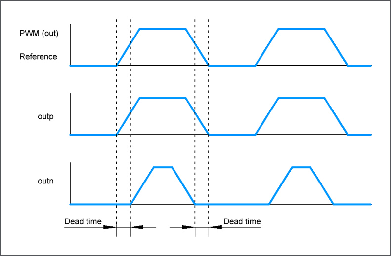
Figure 2 Deadband time OUT- and OUT+